1.5 GHz PLL Frequency Synthesizer
In order to obtain excellent phase stability between two beams in our experiment, it is preferable to derive them from the same laser. This is a limitation however, if the beams operate at different frequencies. For frequency differences of less than a few hunder MHz, the approach is to split the beam and send it through an AOM. For higher frequencies, we employ an optical phase-locked loop (OPLL) in which the beat frequency between two lasers sent to a feedback loop and locked to a given separaion. Since AOMs which opertate at 1.5 GHz have become available, we wanted to explore the phase stability of two beams separated by 3GHz (we send the beam through the AOM twice) derived from the same laser source. In order to to this, we need a low phase noise signal at 1.5 GHz which is to be amplified to 1W (30dBm) ad sent to the modulator. To achieve this we designed a 1.3GHz to 1.7GHz tunable PLL frequency synthesizer, desribed below.
Basic design of PLL synthesiser
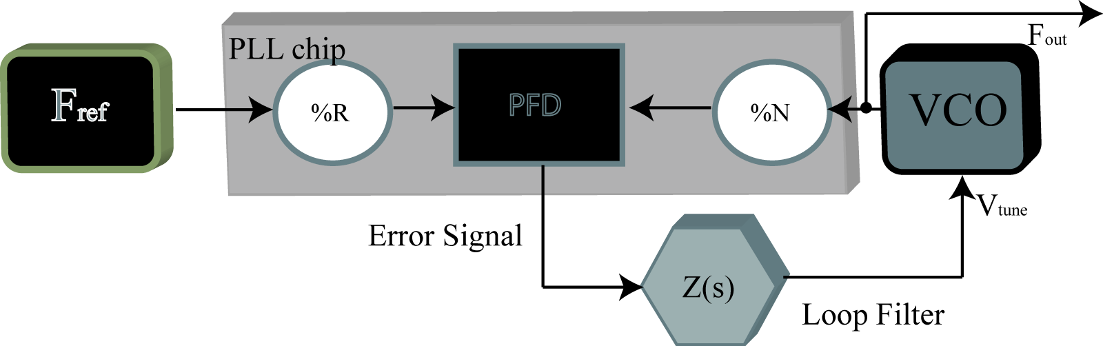
The generic picture of a PLL synthesizer is shown below. Here, everything in grey is typically on an IC, Fref is some stable fixed frequency source, typically a crystal oscillator, or in our case a decent function generator which works up to 20MHz, and VCO is a voltage controlled oscillator capable of operating an RF signal at 1.5GHz. The RF signal is divided down via a prescaler and two separate counters A and B yielding a digital signal with frequency F/N. The reference signal is divided down to a digital signal with frequecy Fref/R. These signals are fed into a Phase Frequency Detector (PFD) containing a charge pump. The charge pump sources current if F/N triggers is first and sinks current if Rref/R comes first producing a digital signal which is integrated to form the error signal. Over time, if F/N is higher then Fref/R, the net result is negative error signal and if F/N is lower then Fref/R, the error signal is positive. This error signal is fed back as the tuning voltage of the VCO, resulting in a stable lock at F = N*Fref/R, corresponding to a constant error signal. The most critical component of the circuit is the loop-filter, which determines the bandwidth of the lock, as well as its overall stability.
Schematic
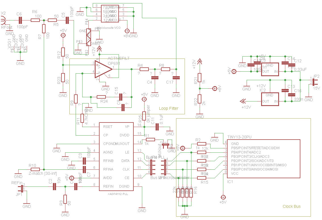
The schematic, designed in Cadsoft EAGLE software is shown below. The frequency source is a minicircuits POS-2000A+ VCO which operates from 1.3GHz to 1.7GHz and has a frequency conversion of about 40 MHz/V. The output is attenuated and sent through an RF power-splitter; one channel leading to the the output via SMA jack, and the other to the PLL. We use an ADF4112 3GHz phase-lock chip from Analog Devices. The device is programed upon start-up by an ATTINY13 microcontroller from ATMEL as descussed later. The feedback loop components are all SMD 1206 packages to minimize stray inductance. The reference signal is input through a BNC jack and AC coupled. On main design challenge is that the VCO needs up to 10V and the PLL itself can only put out about 5.5V. In order to remedy this, the voltage is recentered at around 5V via a low-noise, high slew-rate op-amp (OPA 691). The op-amp can be considered more as a comparater than as a standard negative feedback due to its infinite DC gain, merely extending the volatge range of the charge pump before the integration stage. This is preferable to standard feedback in which the noise of the PLL charge pump is amplified along with the error signal. Since the op-amp inverts the error signal, the charge-pump polarity must be set to negative to compensate. The entire circuit draws about 100mA and is derived from a 15V tabletop supply.
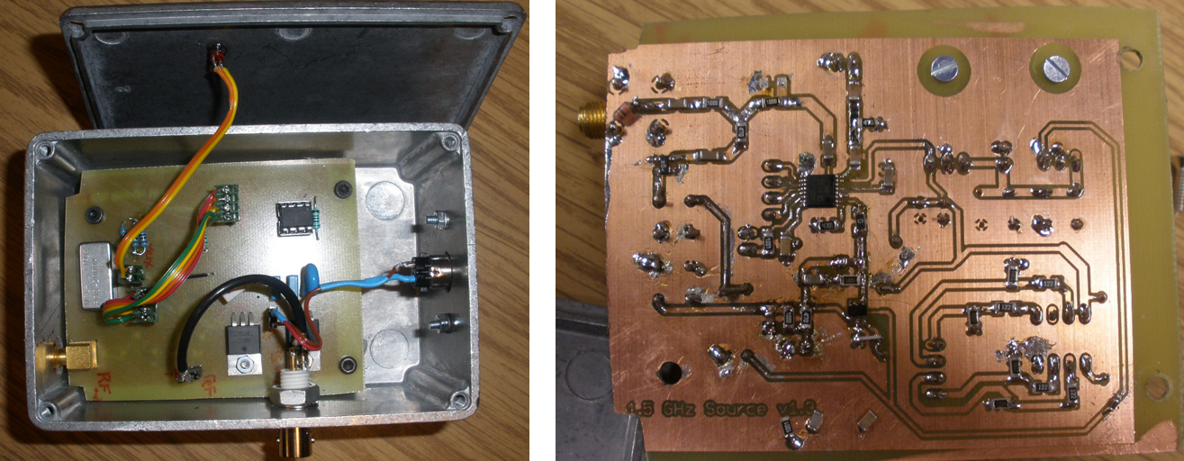
PCB layout and impedance matching
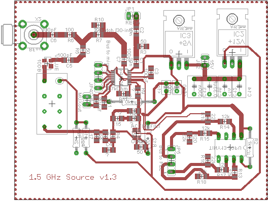
The PCB layout is shown in figure 3. There were several considerations to make due to the high frequency signals involved. First and foremost, the RF lines were kept as short as possible. However, since signal propagation along a copper trace is about c/2 = 1.5 * 10^10 cm/s and the frequency was about 1.5*10^9/s, the half wavelength was about 5cm and so standing wave effect were a concern. For this reason, impedence matching was crucial to approach a near-unity VSWR. It is important to have the trace impedance matched to the input/output impedance of the devices which in this case is 50 Ohm. Given the material of the trace, this can be calculated numerically [1]. A good approximation is given in Dean Banerjee's excellent book [2] to be:
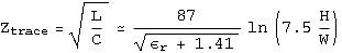 .
.
Here, H and W are height and width respectively. For our board material (FR4) the relative permeability is about 4, yielding a width of W = 2H for 50 Ohm trace impedance. In order to avoid the long power line acting as an antenna, an ferrite bead is used as an rf choke. The power and digital components are spatially separated from the RF components and all supply lines are decoupled from AC via capacitors to ground. The microcontroller bus is connected via a ribbon cable above the board. The entire circuit is housed in an RF shielded case.
Loop Filter
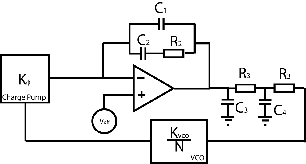
The loop filter determines the overall performace characteristics of the PLL. The basic set-up is as shown in figure 4. The error signal is produced by the charge pump with a gain (usually expressed in mV) Kphi. In the locked condition, the error signal is a DC voltage Vdc corresponding to a frequency around 1.5GHz from the VCO, which for the POS-2000+ from minicircuits, is about 7V. Since the ADF4112 can only put out 5.5V, we need to add a gain stage with an op-amp. The configuration here has infinite DC gain and so acts more like a comparitor at the charge pump output, which is fine as long as the opamp has sufficiently fast slew rate. The output of the gain stage is then sent through a two-pole integreation filter which smooths out the "square-wave" output of the opamp to provide avoltage proportional to the average charge-pump output current. The signal is then sent through the AOM providing gain Kvco(in MHz/V) which is divided by sN to produce the phase error (In the Laplace domain, division by s constitutes integration and phase is the integral of frequency.)
The transfer function of the above loop may be written as [2]:
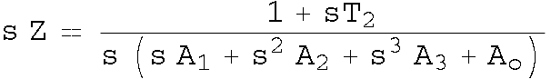
where the various constants are functions of the resistances and capacitances as described in [2]. A calculation in Mathematica is given here, along with the mathematica notebook. The basic idea is to start with the known values for the gain of the VCO (in MHz/V from the datasheet) as well as the gain from the charge pump (which is programmable, see next section,) as well as the desired pole ratios and phase margin for the control loop (47.3 degrees seems to work well.) Given these values you can solve for the various coefficients and then from this, determine the various values of the resistors and capacitors. This procedure can be inverted so that, given a discrete set of components, you can obtain the phase margin and pole ratios etc. This is included in the Mathematica file.
Programming the microcontroller
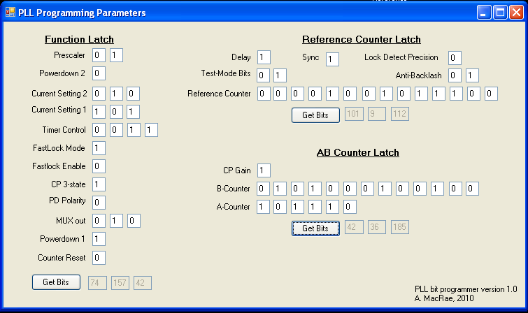
The PLL parameters (loop gain, lock sensitivity, prescaler and conter values, etc) must be programmed upon start up. To accomplish this, we used an ATTINY13 microcontroller (it's what we had laying around.) A good description on how to program such a beast is given here. With the AVR studio, we can program the AVR bitwise in C. A sample program to accomplish this, written by former quantech member J. Appel is given here. From the datasheet, the ADF4112 has a 24 bit register that can be written to its flash memory. Each block determines a group of settings, such as the reference counter and the charge pump gain. The programming occurs by setting bit 1, clocking up and down to read it in, setting bit 2 clocking up and down, and so on all the way to bit 24 after which the 24 bit string is latched and set to memory and you start on the next 24 bits. In order to simplify the programming, a simple program was written to convert the required settings to 3 bytes which are then transferred to the C program. Here are the visual c# project and executable.
Finished Project
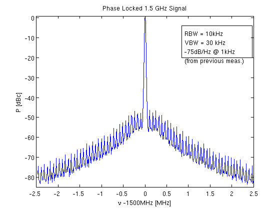
To shield the circuit from external radio-frequency interference and for general protection, the circuit was placed in an conductive case. To run the AOM, we need to amplify the output to 1 Watt (30dBm) without adding to much noise. This is accomplished by a minicircuits ZHL-42 4.2GHz bandwidth RF 30dB amplifier, which has a noise figure of about 7dB (i.e. signal to noise is reduced by a maximum of 7dB after 30 dB of amplification. A final plot of the resultant spectrum is shown below, resulting in a phase noise of less than -70dBc/Hz at 1kHz and a phase varience of less than 10 mrad^2.